QUANTAM TELEMATICS EMPLOYS SOPHISTICATED TECHNOLOGY TO OFFER A UNIQUE FUNCTION SET.
Our customers can define their product requirements to suit their particular environments.
|
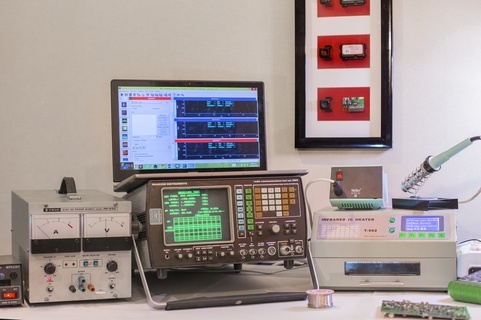 |
Quantam's design centre in New Zealand is equipped to cater for all hardware and firmware aspects of the design. Capabilities include all aspects of analog, digital and RF design. Our RF lab is equipped to cater for frequencies up to 3GHz.
The facility is fully equipped with a bench top SMD placer and reflow oven to manufacture prototypes and evaluation quantities of products for test and sample approval. |
 |
While the team is competent in all aspects of electronic design, when we face complex challenges we are more than happy to take advice from the highly qualified team at one of the local Universities. Isn't it wonderful the freedom age and experience brings? No egos or personal agendas, just a determination to deliver the best product, at the best price, in the shortest possible time. |
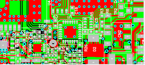 |
Once the basic concepts are in place, CAD forms an integral part of our design process, facilitating all aspects of the products future, from Pick and Place component placement locations through to procurement and inventory management |
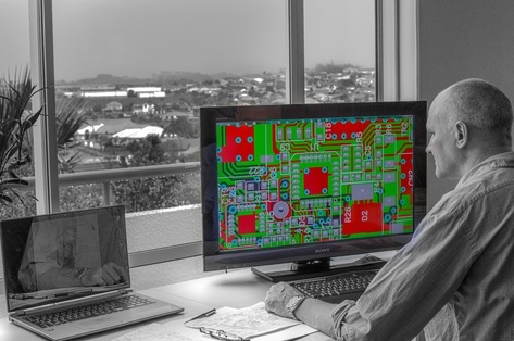 |
A designer scrutinising the CAD files, prior to submission for board manufacture. We have close ties with a competitive PCB supplier in China, offering a 24 hour turn around complete with frame mounted laser cut stainless paste stencil.
|
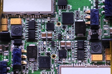 |
An assembled panel of a current design. All our products and services are ROHS compliant. |
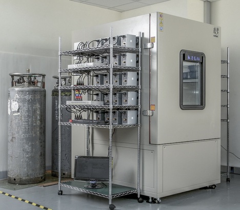 |
Thorough thermal evaluation is completed at our plant in Taiwan. Temperature cycling from -40 C to +120 C is part of our design process. |
|